Project Description
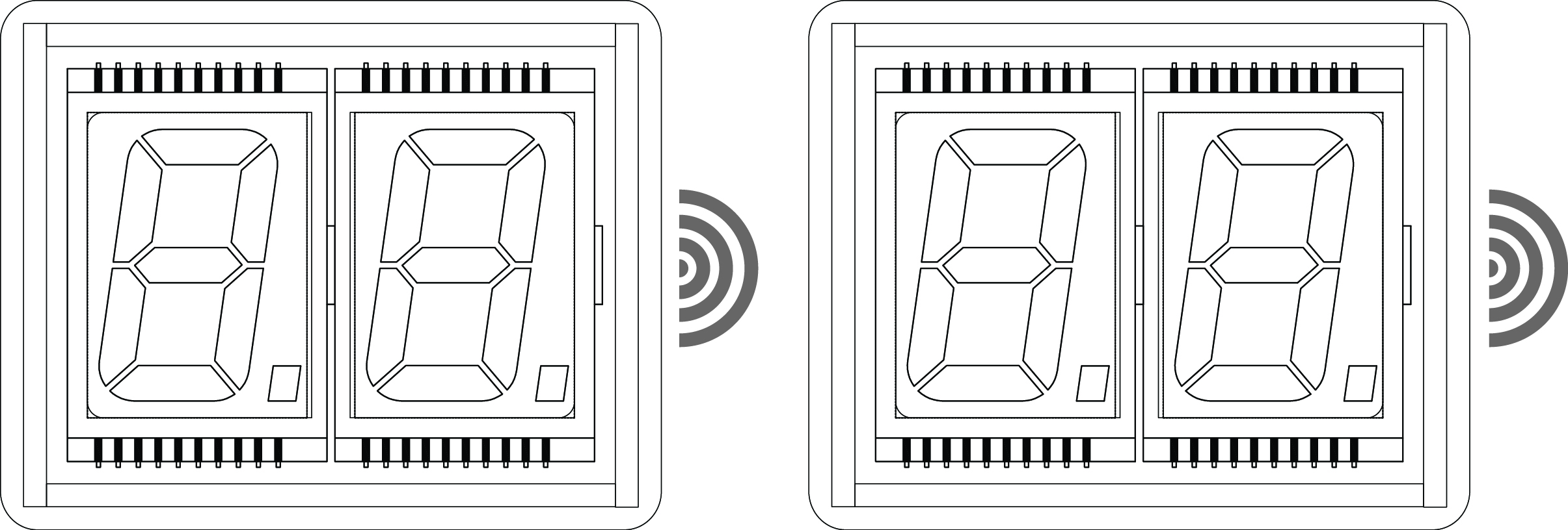
Device is just clock that shows only two digits. Main feature of this clock is that this clock defines order of blocks by itself. Leftmost block always shows hours, next – minutes, third – seconds, fourth – month, fifth – day of month and sixth shows year. Another nice feature that clock has illumination with contact-less button.
Block diagram
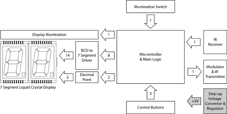
This device contains 9 functional blocks: main block, power supply, IR receiver, IR transmitter, contactless illumination switch, control buttons, display driver, LCD, and illumination.
Hardware
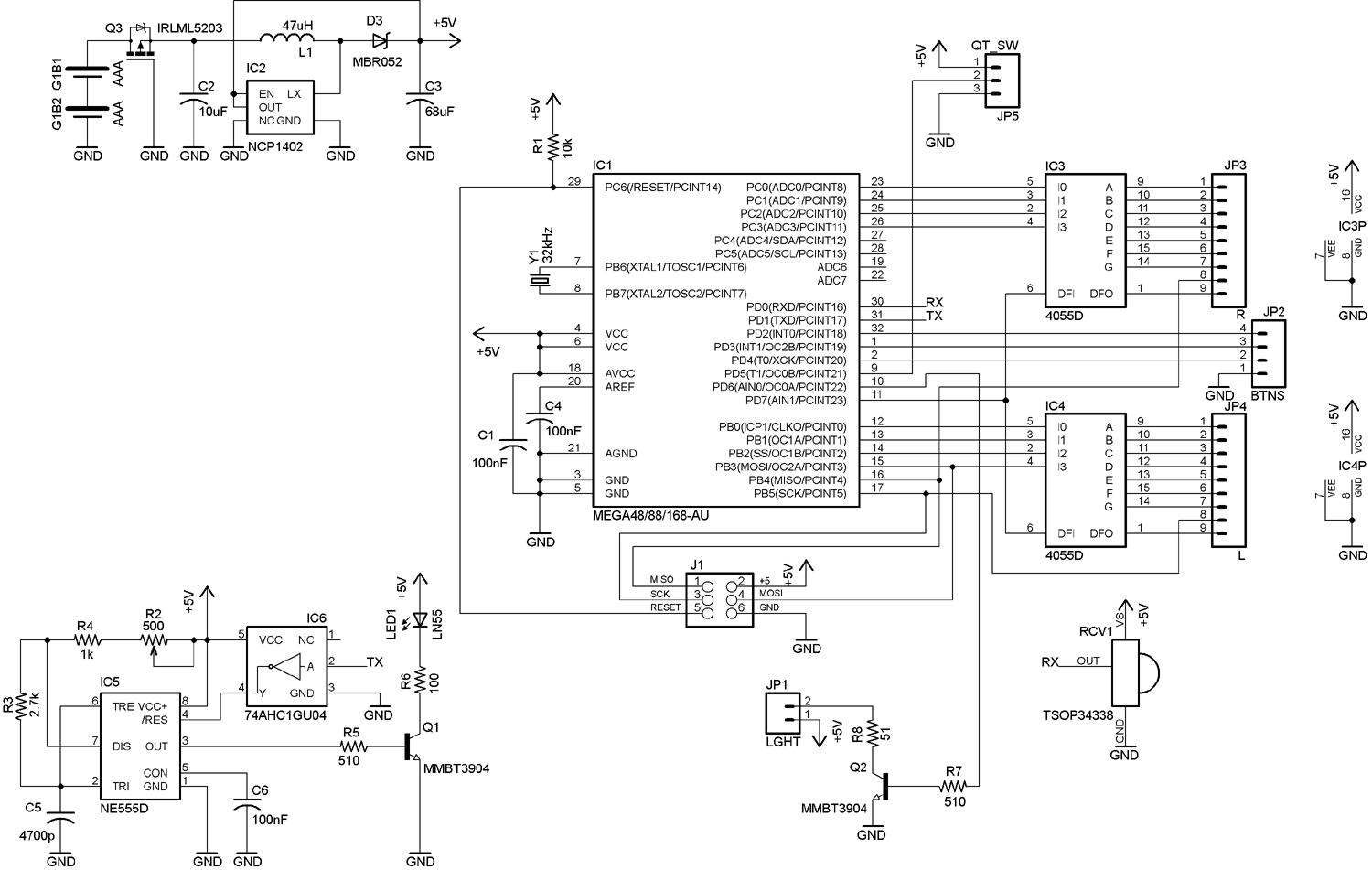
Main block contains microcontroller and defines clock’s behavior and logic. Devices uses Atmel AT Mega 168p 8-bit microcontroller, with internal 1 MHz RC clock. It also uses 32 kHz clock crystal to provide precise time measurement in asynchronous connection. This microcontroller was chosen because of this feature. Using external real-time clock would allow using cheaper micro-controller but would increase device’s total cost. AT Mega 168p also controls all other blocks, IR transmitter and receiver, and display.
Power supply provides 5V supply for device. It uses ON Semiconductor’s NCP1402 step-up convertor. It converts input voltage from 2 AAA batteries as low as 0.8V to constant 5V. Such high power voltage affects power consumption, it is possible to decrease power consumption by just decreasing power voltage down to 3.3V or even 1.8V but liquid crystal display requires 5V so I have to use higher voltage. To prevent battery’s wrong polarity connection power MOSFET (International Rectifier’s IRLML 5103) was used.
Infra-red receiver/transmitter couple used to transfer time and service information between two devices. For preventing light interference and intelligence signal suppression, device uses 38 kHz modulation (or 38 kHz square signal.) When this square signal presented, it means there is intelligence signal. As hardware solution, clock uses simple 555 timer chip and IR light-emitting diode with peak at 950 nm. As IR receiver the clock uses Vishay’s TSOP34338. This device amplifies, filters, and decodes signal modulated with 38 kHz. Main usage is remote for video and audio home electronics but it perfectly suitable for short distance data transmission as well. At first sight it looks like not very stable solution, but it is very tolerant to modulation frequency deviation. Also due high infra-red LED’s consuming current NPN BJT was used in switch mode.
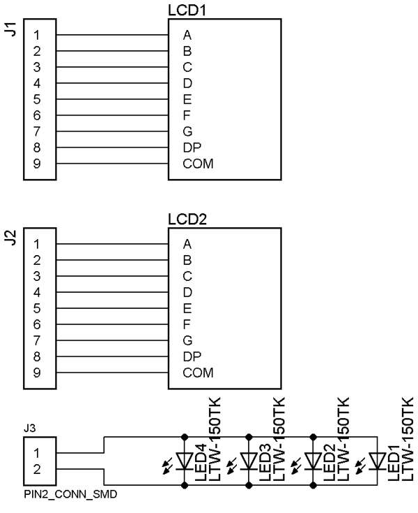
For improving usability the clock uses simple illumination. For illumination purposes simple white light-emitting diodes was used. Initially blue illumination LEDs was planned to use, that supposed to make clock more pretty and cool looking. However experiments showed that regular green LCD has terrible readability with blue color illumination. Design uses 4 diodes in parallel because of forward supply voltage. Each LED has 3.2V forward voltage and 20mA of maximum current. With 4 LEDs in parallel connection we will have 80 mA that exceed maximum current rating of micro-controller’s output pin (about 10 mA.) To prevent chip’s damage clock’s design uses regular NPN BJT, working as switch and providing required current for illumination LEDs.
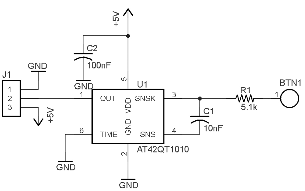
For turning illumination on and off, instead of regular buttons, contactless switch was used. This schematics based on Atmel’s capacitive-touch QT chip series. This chip supposed to creating contactless switch or proximity sensor fairly easy. This contactless switch included in design mostly as experiment than for practical purposes. This technology looks very advanced but easy and cheap.
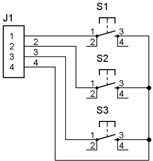
For controlling clock/setting time clock used regular tactile switches control buttons. Control is very simple; there are three tactile switches/buttons, first button used for picking desired part of time (hours/minutes/seconds etc.), second and third to increase and decrease. We can stop at any part of time and clock will show this time as long as there is no ‘master’ clock to the left that sends time.

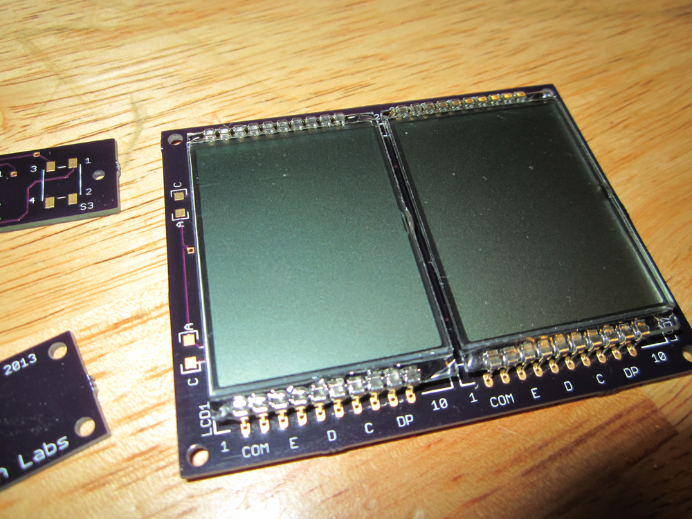
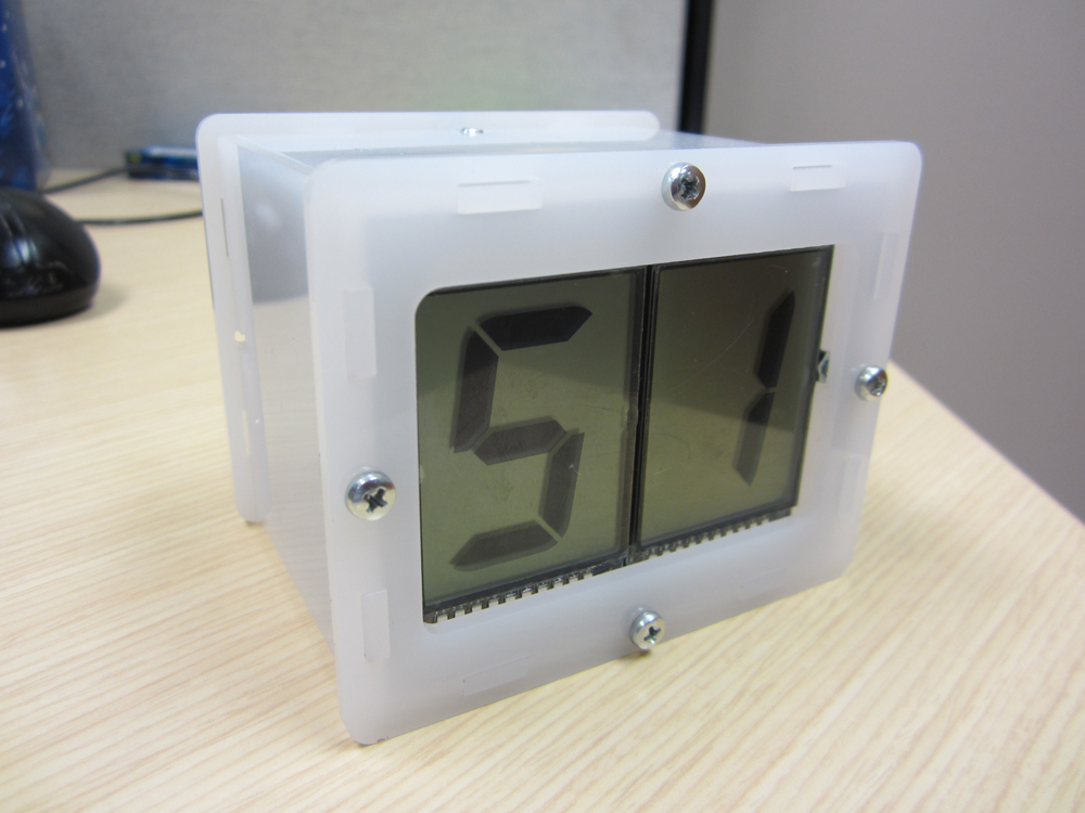
For displaying time two numeric LCD was used. They are relatively big; each one is 2 inches height with 1.36 inches digit. They are pure liquid crystal display so they need special signals. LCD cannot be controlled by DC voltage, in this case liquid crystal will degrade pretty quickly. It should use square signal. To simplify design I used display driver and BCD-to-7-segment conversion chip – Texas Instrument’s CD4055. This is very neat chip, it converts 4 pins BCD into 7 pins output signal with proper signal, that suitable for driving LCD. This piece of silicon also can be used for driving up to 30V display such us vacuum electroluminescent display, even if this is not applicable in this design.
Software
Firmware is written on C programming language using GCC compiler and Atmel Studio as IDE. Code split into two major modules for easier writing and debug: main program and USART library. Main software design is interrupt-driven. There are two main interrupts: asynchronous –for precise time count, controlled by clock crystal and happens every second, synchronous – used as main clock and issues every 1ms (1 kHz). Main 1kHz clock also used for making LCD’s 100 Hz square, constantly redraw display (using polling), send time to next unit (every 5 seconds). Main interrupt set appropriate flag, which are being used in infinite loop in main program.
This design uses mechanical switches, thus there are problem with contacts bouncing. Software debouncing used to resolve this problem. After switching from low to high state on button pin, program waits for 50msec and assumes that contacts’ bouncing is over. After that it waits until contacts are open and uses this moment to engage action (such as increase/decrease time etc.)
For showing time in right order, every unit sends its number, time and date to neighbor at right. If there is another unit, it receives time, sets time and date according to received one and increase unit number, and sends it too. Thus all units synchronize time in respect to leftmost unit and show part according to unit number. To prevent wrong data transmission, every unit also transmits checksum. If checksum does not match with data, unit rejects this transmission and wait for next one. Data are being sent every 5 second to keep good balance between power consumption and response time. Serial transmission uses 300 baud, because data size is very small and we do not need high speed but good reliability.
Design
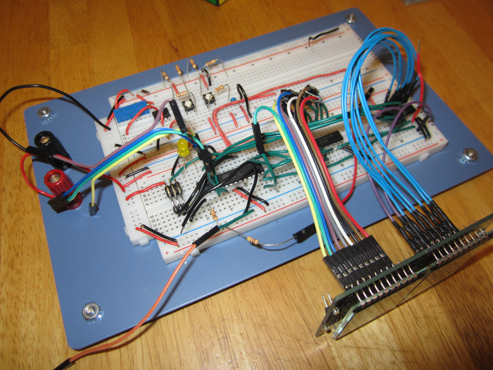
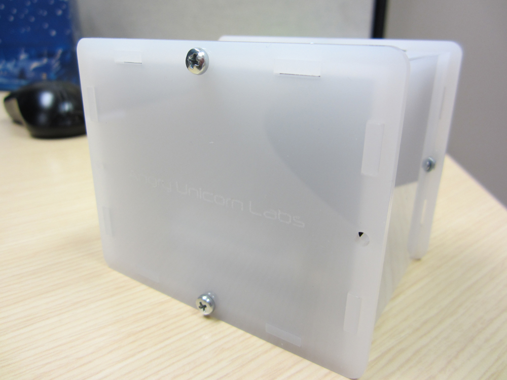
To create accomplished prototype design I designed and ordered enclosure. I used laser-cut acrylic glass. Design was made in Adobe Illustrator and preliminarily cut out of paper to find potential issues. Schematics and print circuit boards were created in Eagle CAD, perfect tool for electronics design. Circuit boards were ordered at 3rd party company who specialize on small batches and perfect for prototyping.
Problems
When I was designing my clock I struggled with few problems. One, most general problem was compatibility problem with lack of time; it was hard to make everything work together. Every time when I debugged one part and added another, both of them stopped working. Careful reviewing showed that I usually forgot to change some small details.
After I soldered first boards I found that QT contactless sensor was over-sensitive. Reading manual revealed that one capacitor affects sensor sensitivity. This chip can be used as proximity sensor with specific values of certain capacitor. I picked average value for this capacitor and it was too high, my finger triggered sensor on distance about 1-2 inches and was too far, so I replaced capacitor. Experimenting with board and sensitivity I re-soldered and killed couple boards and chips, and I have to reorder them so it put even more stress into design process. However, in enclosure, this board is too close to ribbon cables and it interferes to sensor so it keeps illumination constantly on.
Also I made big mistake and trying to reduce cost of parts used software debouncing, instead of hardware one. Adding just on chip per three buttons and three capacitors, I could significantly decrease design time, increasing price less than a dollar. Software debouncing implementation took too much time and didn’t work reliably from beginning.
Big part was designing infrared communication. I never worked with serial port on low level and with infrared communication link too. I found out, by hard way, on my own experience that serial data transfer through IR is hard to debug. Emitter is too powerful and receiver is too sensitive, it makes clock to receive its own signal; they was designed for remote control and for long distances (20-30 ft). If there another transmitter around it messes even more. My protocol was simple, transmit plain data, unit number and time and date data. My attempts to fix it quick were unsuccessful. I need to implement some high level protocol with flow control. For flow control we need bi-directional communication and it requires second serial port. Atmel ATMega has only one hardware serial port. It means we need implement software serial port or use more expensive chip with more ports. Currently, I do not know how implement this yet.
High power consumption, in normal state it takes around 9.8 mA, when transmits data 10.2 mA. When illumination is on, consumption arises to level more than 50 mA. It is possible to reduce power but I did not have time to implement it. With this power consumption clock works about 3-4 day and it is totally unacceptable.
Future advancements
Atomic clock synchronization, automatically reading time from WWVB station Ft Collins, CO on 60 kHz.
- Relatively cheap components ($6).
- Hard to implement, protocol is hard to parse.
- Not reliable reception, complicated error handling.
GPS time synchronization.
- Expensive component ($30-40).
- Easy implementation.
- Reliable reception.
Alarm clock.
Cost
Parts cost me around $100 for 3 prototypes with extra parts. Circuit boards cost about $80 for three. Enclosure costs me about $40 for three.
Conclusion
I was able to build prototype but it was partially successful. It shows time, buttons work, illumination works. However illumination switch is over-sensitive and require re-design both, schematics and enclosure design. Infrared communication surprisingly worked on low level, I was able to transmit stream of data but transmitter high sensitivity messes everything up. However it could be redesigned to new revision.
Schematics
Main board
Contactless sensor
LCD board
Buttons board
Photos

References
- Atmel Corporation. (2013). ATmega 168, 8-bit Microcontroller with 8K Bytes In-System Programmable Flash Datasheet. Retrieved December 2, 2013
- Atmel Corporation. (2013). Atmel AT42QT1011 Single-key QTouch® Touch Sensor IC Datasheet. Retrieved December 2, 2013
- Diodes Incorporated. (2013). NE555/SA555/NA555 PRECISION TIMERS. Retrieved December 2, 2013
- Diodes Incorporated. (2013). 74AHC1GU04 UNBUFFERED SINGLE INVERTER GATE. Retrieved December 2, 2013
- ON Semiconductor. (2013). 200 mA, PFM Step-Up Micropower Switching Regulator. Retrieved December 2, 2013
- Quantum Research. (2013). Secrets of successful QTouch design. Retrieved December 2, 2013
- Texas Instruments. (2013). CMOS Liquid-Crystal Display Drivers datasheet. Retrieved December 2, 2013
- Vishay. (2013). IR Receiver Modules for Remote Control Systems. Retrieved December 2, 2013